Instrumentation
Brillouin-Light-Scattering Spectroscopy
Brillouin Light Scattering (BLS) spectroscopy is based on the detection and the analysis of laser light scattered by fluctuations of refracting index in a medium, caused by phonons. The technique gives access to acoustic or spin waves with frequencies in the range between 3 and 150 GHz. For instance, the acoustic phase velocities of bulk materials and thin films can be estimated. Our experiment is built around a JRS Tandem Fabry-Perot interferometer - Commercial Tandem Fabry-Perot interferometer (The Table Stable). We routinely measure bulk phonons in transparent materials (glassy substrates, crystals, cells, natural materials, etc.) to determine their elastic properties. We also measure surface phonons.
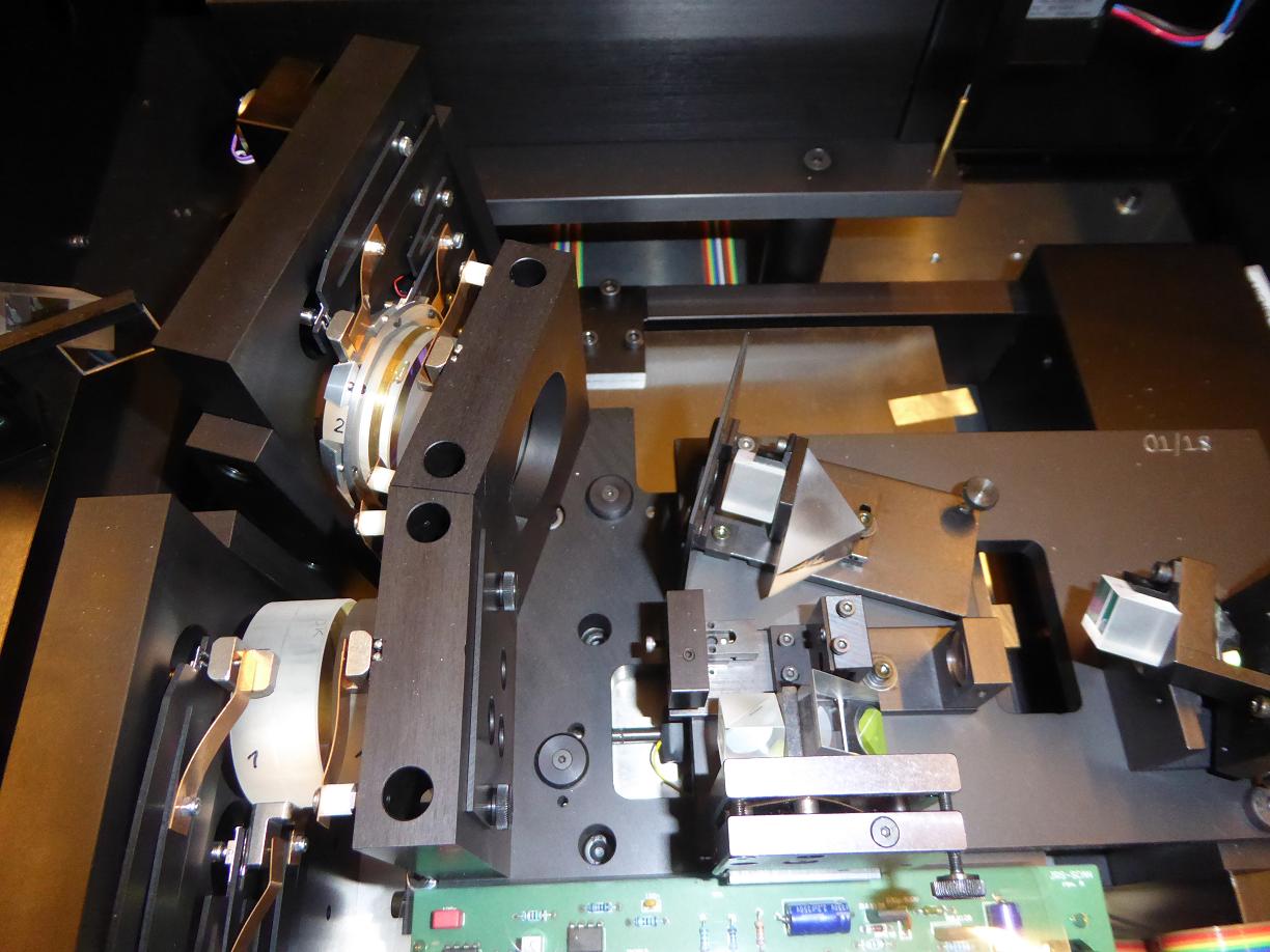
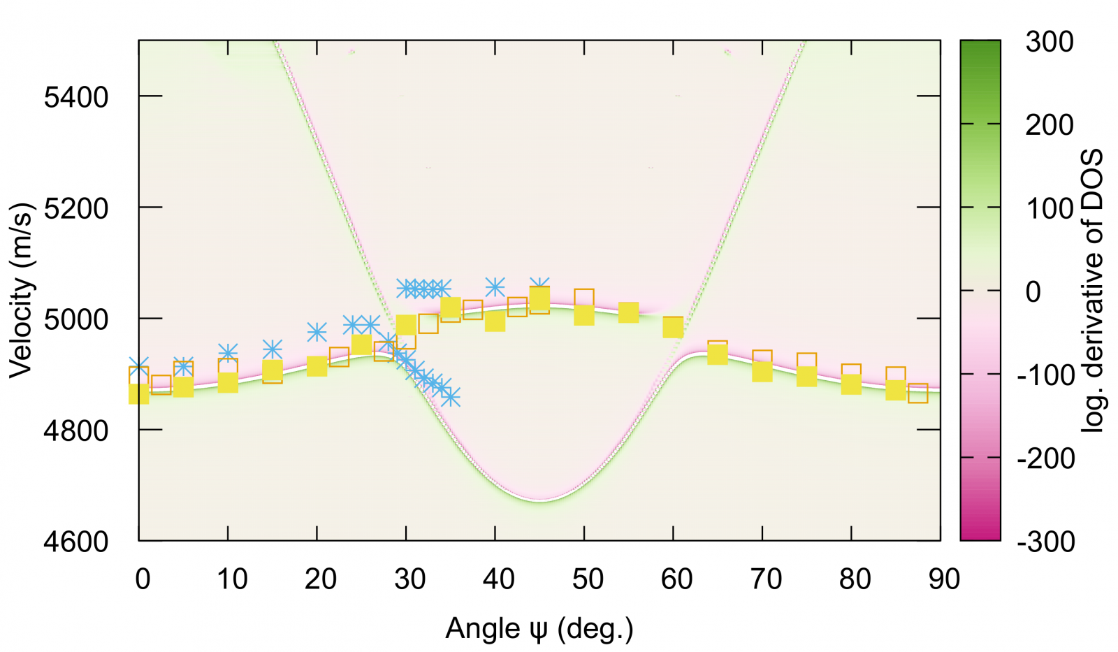
Figure 1: (left) JRS Tandem Fabry-Perot interferometer. (right) Comparison of experimentally determined surface phonon velocity with a resolvent map of the dispersion for surface phonons on the (001) plane of silicon with native oxide.
The PHEMTO platform
The PHEMTO platform (PHEnomènes et Métrologie Thermiques femtOsecondes) uses a double femtosecond Ytterbium:glass laser (t-Pulse Duo model, Amplitude Systèmes) to implement heterodyne pump-probe measurements. Time-resolved thermoreflectance measurements give information on thermal properties (heat conduction, interface resistance) of multilayered samples. The platform also performs picosecond acoustics measurements: the propagation of surface acoustic waves on the surface of the samples can be imaged in time. The acoustic wave velocity in the bulk of the sample can also be obtained by time-of-flight or Brillouin-oscillation measurements.
The platform was designed with LOMA (Laboratoire Ondes et Matière d'Aquitaine) in Bordeaux, France, within the frame of a project funded by ANR (ANR P2N PHEMTO). It was also supported by RTB and CEA-Leti.
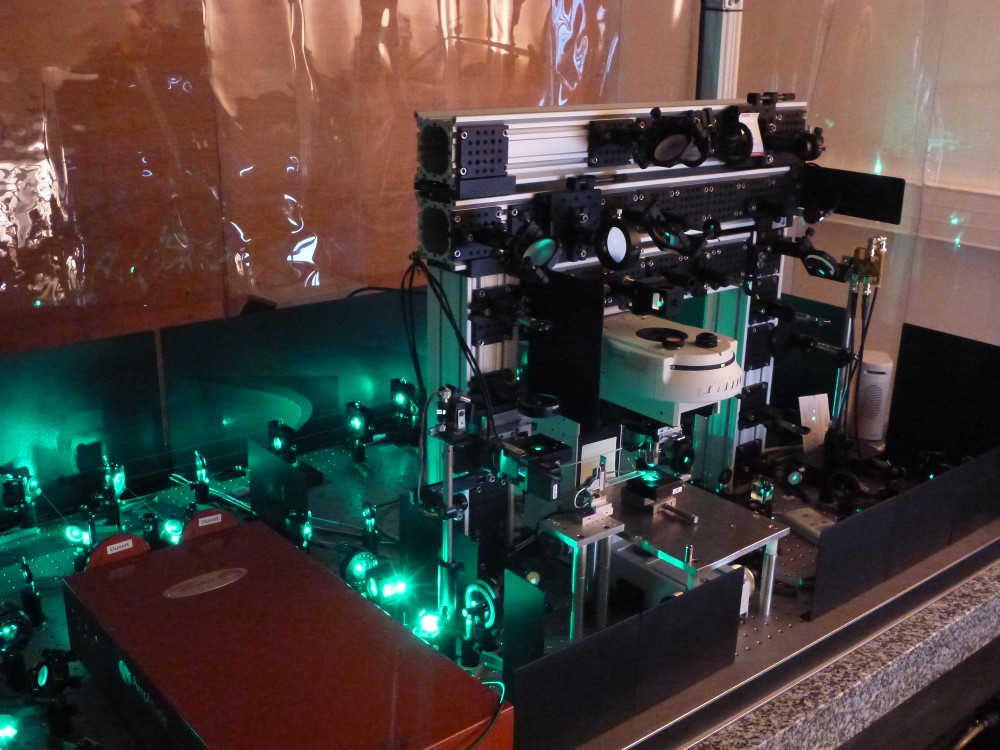
Figure 2: Photograph of the PHEMTO platform in operation
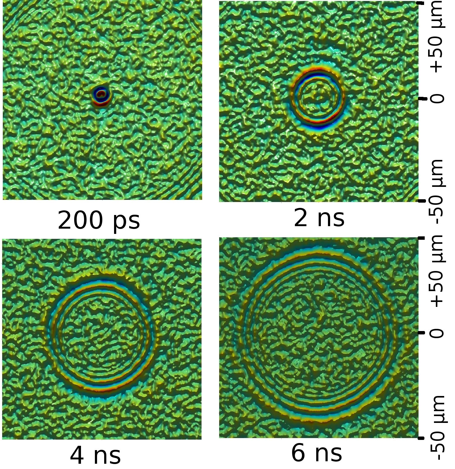
Figure 3: Four snapshots of the formation of surface wave ripples in the first instants following the impact of a pump femtosecond laser pulse. The time delay between each snapshot can be adjusted at will.
Electro-acoustic device characterizations
We are equiped for the electrical characterization of microacoustic devices in the RF frequency range that is typical of wireless communications and SAW/BAW technology. A Süss PM5 manual probe station, associated with an Agilent E5071C vector network analyzer (VNA) allows wafer-level characterizations of electrical and electro-acoustic devices in the 9 kHz - 20 GHz frequency range. Contacted devices can obviously also be characterized using the VNA alone (available calibration kit: Agilent 85033E). Probe station key features:
- 6” vacuum chuck accommodating substrates of 10 mm x 10 mm up to wafers of 150 mm, movement in X, Y, Z, and theta directions, movement range: 155 mm x 155 mm;
- Magnetic PH110 proheads;
- Vibration Isolation Platform VIP600;
- MOTIC PSM1000 microscope, movement range of 50mm x 50 mm, long working distance objectives 2X, 10X, and 20X ;
- 1/2 Color CCD Camera + 15'' TFT monitor.
Currently available probes (other RF probes can be adapted to the PH110 probeheads):
- Cascade Microtech /Z/ Probe Classic (AE-Z10-GS-250 and AE-Z10-SG-250): nickel tips, DC-10 GHz, ground-signal configuration, 250 μm pitch ; associated calibration substrate: CSR-6 50-250 GS/SG.
- GGB Industries Picoprobe (40A-GS-200-P-N and 40A-SG-200-P-N): nickel tips, DC-40 GHz, ground-signal configuration, 200 μm pitch ; associated calibration substrate: CS-8.
Optical heterodyne interferometry
We have developed heterodyne optical intererometrical set-ups allowing to measure elastic vibrations in a variety of devices. The heterodyne operation allows for a self-calibrated measurement of the absolute amplitude of the out-of-plane component of the elastic field. Some of the interferometers have scanning capabilities that allow us to map the surface vibration, hence providing us with a more precise picture of wave propagation at the surface of the investigated sample, including losses or energy distribution. A unique advantage of this imaging method is that each potentially excitable wave can be interrogated individually by scanning the input frequency and mapping the induced spatial surface amplitude distribution. The interferometrical set-ups therefore grant us access to information that cannot be obtained by simple electro-acoustic characterizations of the devices alone.
The interferometers are suited for absolute amplitude measurements up to 12 GHz for bulk acoustic wave devices. The spatial resolution is of the order of 1 µm.

Figure 4: Optical characterizations of a phononic waveguide device with an eight-period long crystal consisting of a square lattice of air holes etched into lithium niobate. The measured elastic wave field amplitude maps correspond to excitation frequencies located (a) and (b) inside (712 and 820 MHz) and (c) at the output (940 MHz) of the band gap.

